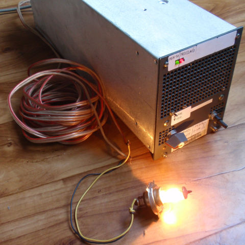
This switching power supply was built because I needed a powerfull adjustable bench power supply. Linear topology would be unusable for this power
(2400W = 2.4 kilowatts!), so I chose a switching topology of a two switch forward (half-controlled bridge).
In my article about SMPS's it is a topology II.D. The switching supply uses IGBT transistors and is controlled by UC3845 chip.
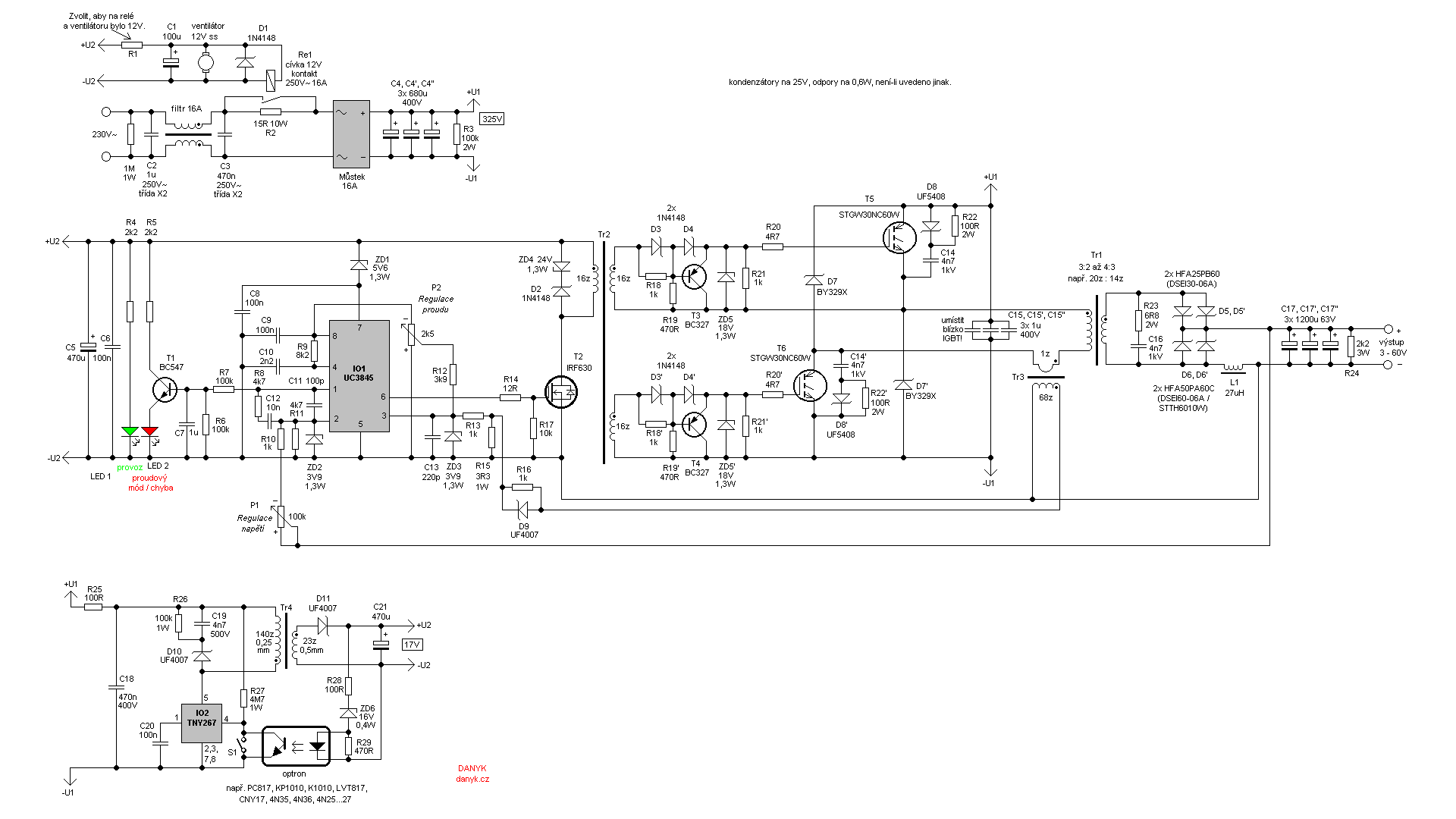
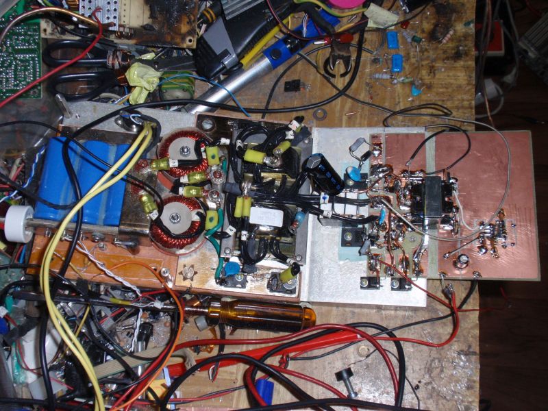
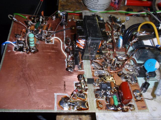
The schematic of my switching power supply you can see below.
Mains voltage goes first through an EMI interference filter. It is then rectified using a bridge rectifier and smoothed using capacitor C4.
Due to high capacity, there's an inrush limiting circuit with Re1 relay contact and R2 resistor. Relay coil and fan (from an AT / ATX PC power supply)
are powered from 12V, which is dropped from 17V aux supply using a resistor R1. Select R1 value so that the voltage at the relay coil and the fan was 12V.
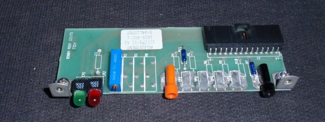
The auxiliary power supply circuit uses TNY267. It is similar to
a power supply described here. R27 provides undervoltage protection of auxiliary power - it will not turn on at less than 230V DC.
UC3845 control circuit has the output frequency of 50kHz and 47% maximum duty cycle. It is powered through the zener diode, which reduces the supply voltage
by 5.6 V (ie to 11.4 V) and also shifts the UVLO thresholds of 7.9 V (lower) and 8.5 V (upper) to 13.5 V and 14.1 V. The UC3845 chip then begins to work at
14.1 V and never runs below 13.5 V, which protects the IGBT transistors from desaturation. The original UVLO thresholds of UC3845 are simply too low.
The chip controls the MOSFET T2, which drives the gate-drive transformer Tr2. It provides galvanic isolation and floating drive for upper IGBT.
Via shaping circuits with T3 and T4 it drives gates of IGBTs T5 and T6. They then switch rectified mains voltage (325V) to power transformer
Tr1. Its output is then rectified and finally averaged by inductor L1 and smoothed by capacitor bank C17. Voltage feedback
is connected from the output to pin 2 of IO1. The output voltage of the power supply can be set using the potentiometer P1. Galvanic isolation of the feedback is not necessary
because the control circuit is connected to the secondary SMPS side and isolated from the mains. Current feedback is fed through the current
transformer TR3 into pin 3 of the UC3845 chip. The threshold current of the overcurrent protection can be set by P2 potentiometer.
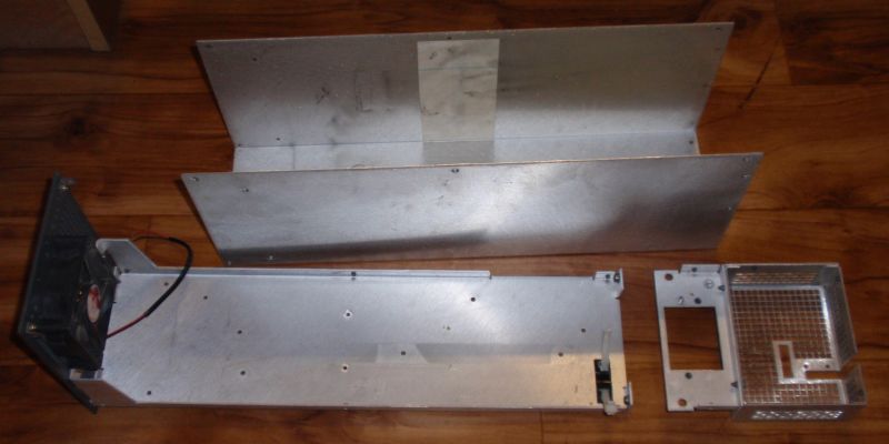
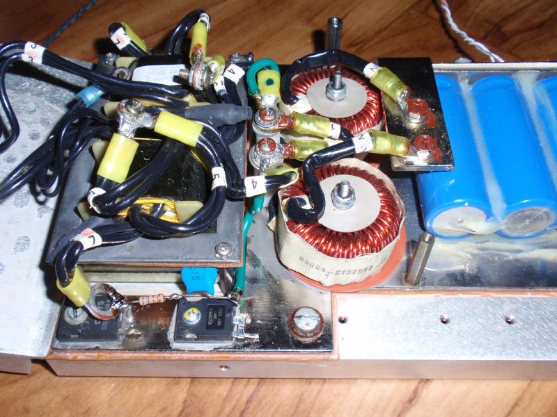
Transistors T5 and T6, diodes D5, D5', D6, D6', D7, D7', and the bridge should be placed on the heatsink.
Diodes D7, capacitor bank C15 and protective RDC snubbers R22 + D8 + C14 should be placed as close as possible to the IGBTs. LED 1 indicates operation of the power supply,
LED 2 indicates the current limiting mode (overload / short circuit) or error. It lights up when the supply is not working in voltage mode. In voltage mode, on the
pin 1 of IO1 there's 2.5 V, otherwise it is about 6V. The LEDs can be omitted.
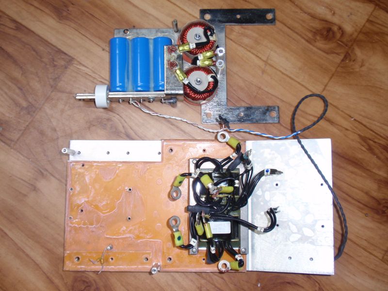
Inductances: Power transformer Tr1 I've salvaged from an old powerfull 56V switched power supply.
Transformation ratio of primary to secondary is about 3:2 to 4:3 and the ferrite core (EE shape) has
no air gap. If you like to wind it yourself, use a similar core as I used in my welding inverter,
about 6.4 cm2 (acceptable range is 6-8 square cm). The primary is 20 turns of 20 wires, each has diameter of 0.5 to 0.6 mm. The secondary is 14 turns
of 28 wires together, of the same diameter as primary.
It is also possible to make windings of copper strips. On the contrary, the use of a single thick wire is not possible because of the skin effect (as it works with high
frequencies). Splitting the winding is not required, you can for example wind primary first and then secondary.
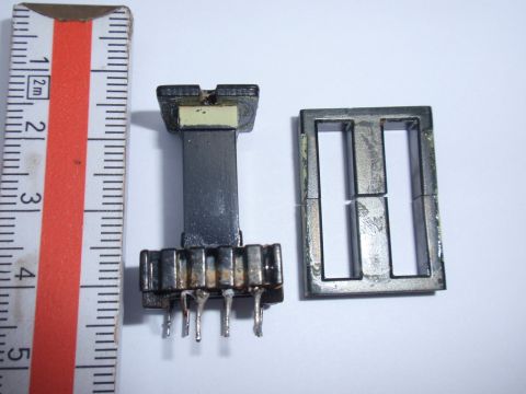
Forward gate-drive transformer Tr2 has three windings, 16 turns each. All winding are wound at once, using three twisted insulated bell wires. Is is wound
on an EI ferrite core (EE can also be used) without air gap. I salvaged it from the main power transformer from an ATX or AT computer power supply.
The core has a cross section of about 80 to 120 mm2.
Current transformer TR3 has 1 turn primary and 68 turn secondary on a ferrite or iron poweder ring and the size or number of turns is not critical.
In case of different number of turns you have to adjust R15.
Auxiliary power transformer TR4 is wound on ferrite EE core with air gap and the cross section about 16 to 25 mm2.
It comes from the auxiliary power transformer taken from an old ATX. Orientation of windings of transformers (marked by dots) must be followed!
Double winding EMI filter can be eg from a microwave oven. Output coil L1 also comes from the 56V SMPS I've taken apart.
It consists of two parallel inductors 54uH on the iron powder rings and the total inductance is therefore 27uH.
Each coil is a wound by two magnet copper wires, 1.7 mm diameter each. The total cross section of L1 windings is then approximately 9 mm2.
L1 is connected to the negative branch, so the cathodes of diodes have no RF voltage on them
and so they can be mounted on a heat sink without insulation. Maximum input power of this switched power supply is about 2600W and
efficiency at full load more than 90%.
In this switching power supply I used STGW30NC60W IGBTs. They can be replaced by the types IRG4PC40W, IRG4PC50W, IRG4PC50U,
STGW30NC60WD or similar enough powerful and fast ones rated for 600V. The output diodes can be any ultrafast ones with enough current rating. The upper diode (D5) sees
20A average current in the worst case, the lower diode (D6) sees 40A in the worst case. The upper diode thus can be rated for half the current of the bottom diode.
The upper diode can be eg two parallel HFA25PB60 / DSEI30-06A or single DSEI60-06A / STTH6010W / HFA50PA60C. Bottom diode may be two parallel
DSEI60-06A / STTH6010W / HFA50PA60C or four HFA25PB60 / DSEI30-06A.
The heatsink of the diodes must dissipate approximately 60W. Power dissipation of IGBTs can be up to 50W.
The dissipation of D7 diodes is difficult to predict because it depends on the properties of Tr1 (its inductance and coupling).
The dissipation of the bridge rectifier is up to 25W. This power supply uses a very similar schematic as my welding inverter,
since it works really well.
Switch S1 allows standby shutdown. This is useful so you don't always have to switch the mains input of this powerful power supply.
Consumption in the standby state is only about 1W. S1 can be omitted. This power supply can also be constructed for a
fixed output voltage. In this case it is advisable to optimize the transformation ratio of Tr1 for the best efficiency
(eg, primary has 20 turns and the sedondary has 1 turn per every 3.5 - 4V of output voltage).